File:Electron density wave - plasmon excitations.png
此为最大尺寸。
Electron_density_wave_-_plasmon_excitations.png (666 × 199像素,文件大小:2 KB,MIME类型:image/png)

|
此diagram图片可使用矢量图形重新创建为SVG文件。这具有很多好处;更多信息请参见共享资源:待清理媒体。如果存在此图片的SVG格式,请将其上传,然后将此模板替换为
{{vector version available|新图片名称}}。
建议您将SVG命名为“Electron density wave - plasmon excitations.svg”,这样在使用Vector version available(或Vva)模板时就不需要填写新图片名称参数。 |
摘要
| 描述 |
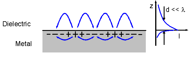
English: Schematic representation of an electron density wave propagating along a metal/dielectric interface. The charge density oscillations and associated electromagnetic fields are called surface plasmon-polariton waves. The exponential dependence of the electromagnetic field intensity on the distance away from the interface is shown on the right. These waves can be excited very efficiently with light in the visible range of the electromagnetic spectrum.
Presently, metallic nanostructures are used to fabricate/analyze:
|
| 日期 | |
| 来源 | National Science Foundation - Center for Probing the Nanoscale |
| 作者 | Center for Probing the Nanoscale - |
| 授权 (二次使用本文件) |
Public Domain - NSF (of US government) |
许可协议
此作品在美国属于公有领域,因为其是由美国政府的官员或雇员,基于其个人公务目的制作的作品,参考美国法典第17篇第1章第105条。
注意︰本模板仅适用于美国联邦政府的原创作品,不适用于任何美国州、属地、联邦个体、县、市或任何次级政府的作品。本模板也不适用于1978年以后由美国邮政署出版的邮票图案(参看美国版权局实践纲领第313.6(C)(1)条)。也不适用于部分美国硬币;参看美国铸币局使用条款。 |
 | |
| 本文件已被确认为免除已知的著作权法限制(包括所有相关权利)。 | ||
文件历史
点击某个日期/时间查看对应时刻的文件。
| 日期/时间 | 缩略图 | 大小 | 用户 | 备注 | |
|---|---|---|---|---|---|
| 当前 | 2010年8月1日 (日) 15:41 | 666 × 199(2 KB) | Dbc334 | == {{int:filedesc}} == {{Information |Description={{en|1=[http://www.stanford.edu/group/cpn/research/investigators_2.html Schematic representation] of an electron density wave propagating along a metal/dielectric interface. The charge density oscillations |
文件用途
以下页面使用本文件:
全域文件用途
以下其他wiki使用此文件:
- ar.wikipedia.org上的用途
- ca.wikipedia.org上的用途
- en.wikipedia.org上的用途
- es.wikipedia.org上的用途
- fr.wikipedia.org上的用途
- ja.wikipedia.org上的用途