File:CMOS NAND Layout.svg

此 SVG 檔案的 PNG 預覽的大小:294 × 587 像素。 其他解析度:120 × 240 像素 | 240 × 480 像素 | 384 × 768 像素 | 513 × 1,024 像素 | 1,025 × 2,048 像素。
原始檔案 (SVG 檔案,表面大小:294 × 587 像素,檔案大小:12 KB)
摘要
| 描述 |
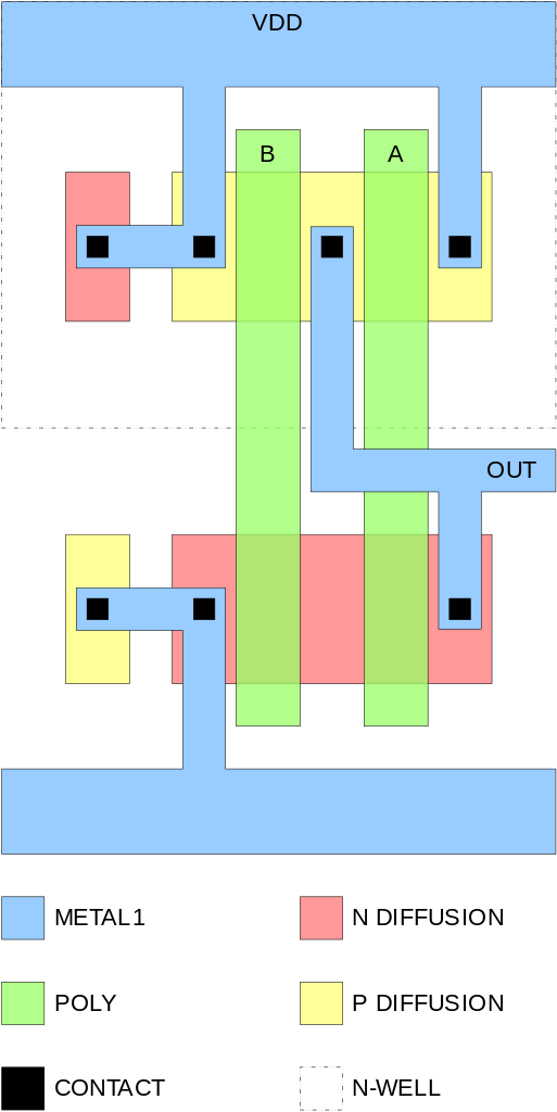
English: The physical layout of a CMOS NAND circuit. The larger regions of N-type diffusion and P-type diffusion are part of the transistors. The two smaller regions on the left are taps to prevent latchup.
עברית: שער לוגי מסוג NAND ממבט על.
Polski: budowa bramki NAND CMOS.
Română: Aranjamentul fizic al unei porţi NAND CMOS.
中文:CMOS与非门的布图. CMOS NAND Layout for chip |
| 日期 | 2006年九月7日 (原始上傳日期) |
| 來源 | Transferred from en.wikipedia to Commons. |
| 作者 | 英文維基百科的Jamesm76 |
| 其他版本 | Derivative works of this file: CMOS AND Silicon.svg |
授權條款
| 此作品已由其作者,英文維基百科的Jamesm76,釋出至公有領域。此授權條款在全世界均適用。 這可能在某些國家不合法,如果是的話: Jamesm76授予任何人有權利使用此作品於任何用途,除受法律約束外,不受任何限制。 |
原始上傳日誌
The original description page was here. All following user names refer to en.wikipedia.
- 2006-09-07 23:46 Jamesm76 294×587×0 (11839 bytes) I am the author and I release this to the public domain.
- 2006-09-07 23:27 Jamesm76 294×587×0 (11827 bytes) SVG drawing of a CMOS NAND gate replacing the older PNG version I had previously uploaded ("CMOS NAND Layout.png"). I am the author and I release this to the public domain.
檔案歷史
點選日期/時間以檢視該時間的檔案版本。
| 日期/時間 | 縮圖 | 尺寸 | 用戶 | 備註 | |
|---|---|---|---|---|---|
| 目前 | 2007年10月19日 (五) 20:46 | | 294 × 587(12 KB) | Prolineserver | {{Information |Description=''no original description'' |Source=Originally from [http://en.wikipedia.org en.wikipedia]; description page is/was [http://en.wikipedia.org/w/index.php?title=Image%3ACMOS_NAND_Layout.svg here]. |Date=2006-09-07 (first version); |
檔案用途
下列頁面有用到此檔案:
全域檔案使用狀況
以下其他 wiki 使用了這個檔案:
- ar.wikipedia.org 的使用狀況
- az.wikipedia.org 的使用狀況
- ca.wikipedia.org 的使用狀況
- en.wikipedia.org 的使用狀況
- en.wikibooks.org 的使用狀況
- en.wikiversity.org 的使用狀況
- es.wikipedia.org 的使用狀況
- fr.wikipedia.org 的使用狀況
- fr.wikiversity.org 的使用狀況
- he.wikipedia.org 的使用狀況
- hi.wikipedia.org 的使用狀況
- ja.wikipedia.org 的使用狀況
- ko.wikipedia.org 的使用狀況
- pl.wikipedia.org 的使用狀況
- ro.wikipedia.org 的使用狀況
- sh.wikipedia.org 的使用狀況
- sr.wikipedia.org 的使用狀況